This was a solo project where I designed a wearable wireless audio system which allows audio passthrough for cosplayers who cannot hear due to large costume peices. This gave me the opportunity to take a PCB from concept to production and develop firmware supporting bluetooth communication. I was able to send the design to JLCPCB and pay to have it manufactured, as well as have the surface mount components soldered on (this would have been extremely difficult to do by hand as many of the passive components were very small in order to it into the small package).
Early Concepting
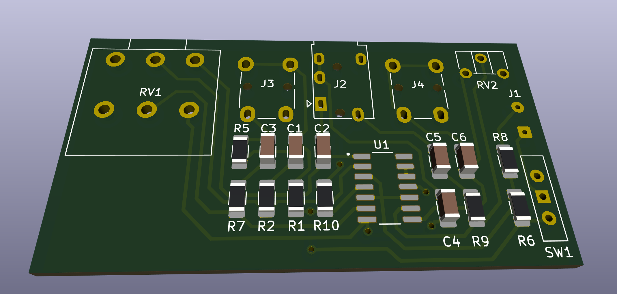 The first design for the board consisted simply of three audio jacks (mic in, speaker out, and headset in/out), two potentiometers (for controlling volumes), and an LM124DR operational amplifier (as well as some passives and power input + switch).
This was the baseline for what I wanted the project to achieve, amplifying external audio for the headset, and amplifying the headset mic for external speakers.
But this project was going to show me just how easy it was for scope to creep out of control.
The first design for the board consisted simply of three audio jacks (mic in, speaker out, and headset in/out), two potentiometers (for controlling volumes), and an LM124DR operational amplifier (as well as some passives and power input + switch).
This was the baseline for what I wanted the project to achieve, amplifying external audio for the headset, and amplifying the headset mic for external speakers.
But this project was going to show me just how easy it was for scope to creep out of control.
Final Features
The problem with self guided projects which take time, is I keep thinking of new things to add. In the end the design had:
- Two seperate WM8988 audio amplifier chips with digital audio input and output
- an ESP32 wireless microcontroller for playing audio, controlling volume, and interfacing with the other peripherals
- a USB-C port for power and microcontroller programming
- Two 5-pin generic connectors for future expansion boards over I2C
- A 3-pin connector for WS2812 addressable LED control
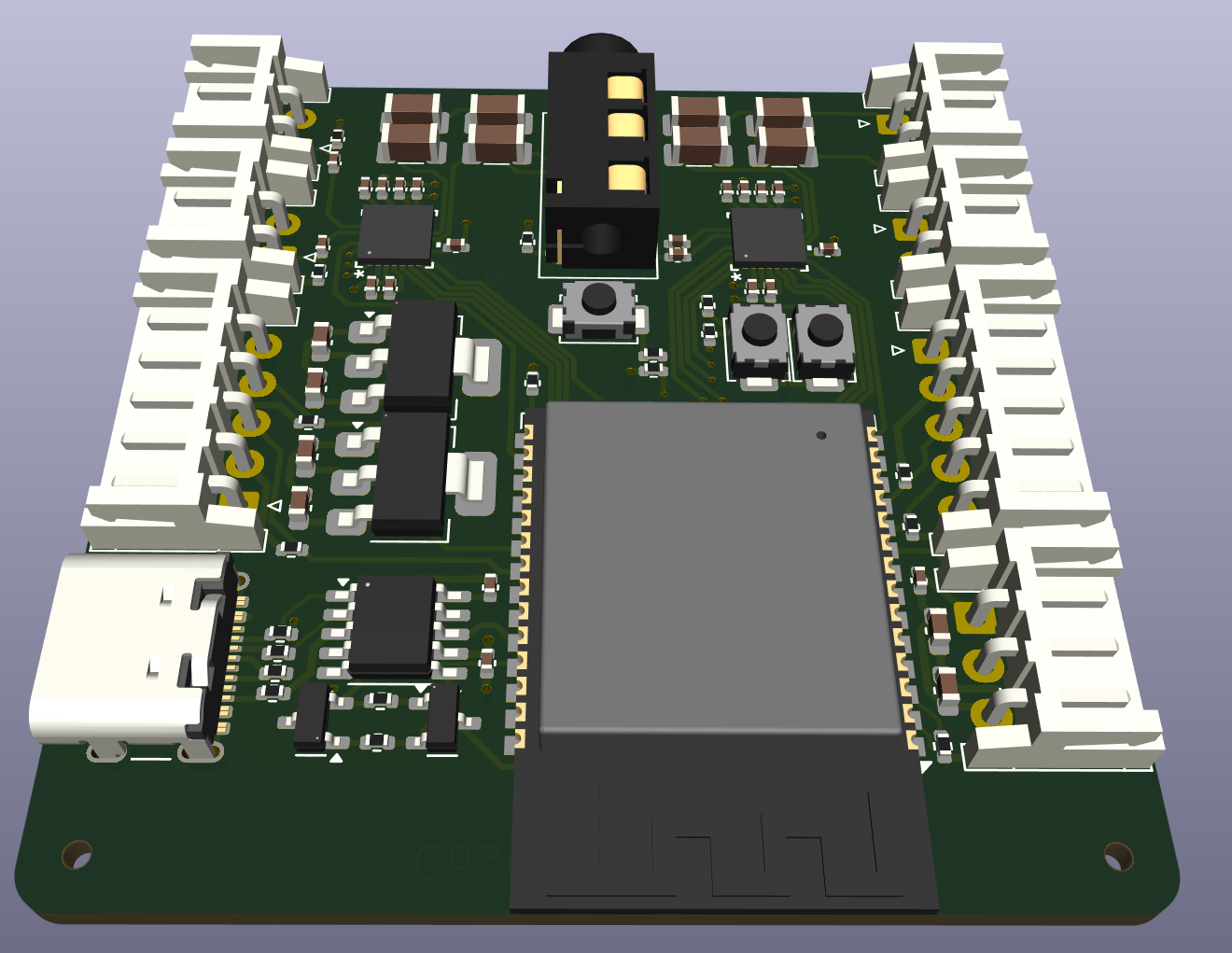 I set a requirment for the board to be no larger than 50x50mm to make the design easier to incorporate into costumes.
This meant highly condensed routing and very small passive component footprints, and to make this possible I increased the number of coppper layers from 2 to 4 to allow 3.3V and 5V fill planes as well as a ground plane and signal layer.
The power and ground planes are split into analogue and digital sections to prevent digital noise from interfering with the audio signals.
This is why there are two linear regulators, to help isolate the power domains.
I set a requirment for the board to be no larger than 50x50mm to make the design easier to incorporate into costumes.
This meant highly condensed routing and very small passive component footprints, and to make this possible I increased the number of coppper layers from 2 to 4 to allow 3.3V and 5V fill planes as well as a ground plane and signal layer.
The power and ground planes are split into analogue and digital sections to prevent digital noise from interfering with the audio signals.
This is why there are two linear regulators, to help isolate the power domains.
Production
To actually have the design made, I uploaded the generated gerber files, bill of materials, and part placement files to JLCPCB, and they provided a quote for both PCB manufacturing and SMD component assembly. The price of manufacturing the PCB was significantly lower than the price of SMD assembly due to the high setup costs for non-standard parts like the audio chips and microcontroller. This makes prototyping somewhat expensive for hobbyists, but on large orders, the price will approach cost of components.
For the through hole and external components such as speakers, mics, and cables, I ordered these from LCSC.com using the bill of materials generated by KiCad.
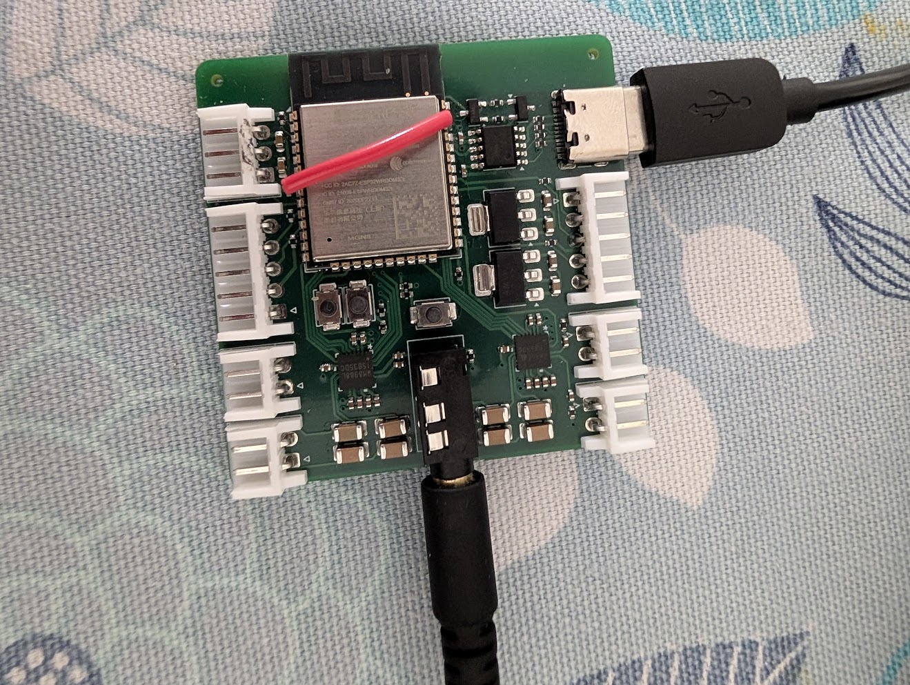 As you can see from the wire across the microcontroller in the picture above, I made mistakes in design of the PCB. Luckily, all of these issues could be worked around with some difficult soldering and programming.
The first issue I encountered is I was not able to upload code onto the microcontroller. It turns out I had unknowingly used a strapping-pin as a digital audio input from one of the audio chips. During startup, the audio chip pulled this input high which told the microcontroller to run the flash memory at 1.8V as opposed to the standard 3.3V. This made the flash non-functional, which would have been catastrophic if it werent for eFuses. I was able to configure the microcontroller to ignore the state of the strapping pin and always use 3.3V flash voltage.
The second issue was I had used 2 input-only pins as outputs to the audio chips, to solve this I had to solder wires across the top of the microcontroller to connect the traces to output capable pins. The final issue was that I had simply forgotten to draw traces beween some parallel capacitors, which was fixable by creating a solder bridge between them.
Programming it
This part is pretty boring, I just had to write code which sent commands over SPI to turn on the audio chips and configure their volume and mixing. I also experimented with using bluetooth communication, and was able to get audio playing from my phone, however I discovered that bluetooth low energy (BLE) which is used for sending commands, is extremely complicated, and not even Claude could get it to work. I eventually resorted to using sending full serial commands over bluetooth classic, which was easy to implement, but you could actually hear it interfering with the bluetooth audio when sending commands at the same time as playing audio.
Conclusion?
While this project was plagued with design mistakes on my part (which I could have easily avoided if I had paid more attention to the built in KiCad rules checker tools), it gave me experience with designing a relatively complex electronic circuit to fit into a small package. The most valuable lesson from this was seeing how easy it was to sink a decent sum of money into manufacturing a defective design! I was fortunate that I was able to solve all the issues (great experience in diagnostics), however in the end I had been overestimating the quality of tiny audio chips and tiny microphones, and the resulting sound quality was pretty terrible. If I were to solve this, I would likely have to add preamps to the microphones, or use bigger better microphones.
It was a good thing I added that addressable LED port, because now I can repurpose the 5 boards I had made into WLED controllers to make my house sparkly and rainbow!